
Huawei’s newest semiconductor claim is not just about making chips smaller. It is an attempt to move the industry’s scoreboard away from foundry node names and toward a metric China may have more room to control: how quickly signals and data move through a chip system.
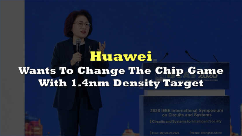
At the 2026 IEEE International Symposium on Circuits and Systems in Shanghai, He Tingbo, president of Huawei Semiconductor and director of the company’s Scientist Committee, presented what Huawei calls the Tau Scaling Law. The company frames it as a replacement for geometry-led scaling, the long-running industry model that tied chip progress to shrinking transistors.
The strategic claim is simple but loaded: if chip performance is increasingly limited by delay, wiring, data movement, and system coordination, then the next race may not be won only by the company with the smallest printed node. Huawei is arguing that progress can also come from compressing signal-propagation time across devices, circuits, chips, and computing systems.
 Sponsored · Altamira Gold Corp.
Huawei says high-end chips based on Tau Scaling are expected to reach transistor density equivalent to 14 Å, or 1.4nm, processes by 2031.
“Equivalent” density lets Huawei compare future designs against advanced-node benchmarks without proving that it has matched Taiwan Semiconductor Manufacturing Company, Samsung, or Intel in conventional lithography. It also gives Huawei a way to describe progress in terms of realized design density and system performance rather than direct access to the most advanced chipmaking equipment.
The near-term proof point is LogicFolding, a Huawei architecture designed to shorten critical-path wiring and reduce signal delay. Huawei said new Kirin chips scheduled for Fall 2026 will be the first to use the architecture.
Huawei says Tau Scaling works across four layers. At the device level, it targets resistance and parasitic capacitance. At the circuit level, it uses LogicFolding. At the chip level, it coordinates software, architecture, and silicon design. At the system level, it points to UnifiedBus, which Huawei says supports unified memory addressing and lower communication latency in SuperPoDs.
 Sponsored · Cambria Gold Mines
The company also said 381 chips have been designed and mass-produced over the past six years using Tau Scaling. The ISCAS abstract separately says Huawei’s exploration covers more than 150 advanced chips or over 150 designs, a difference that is not explained in the public materials.
Huawei’s claim arrives while the global leading edge is still advancing. TSMC says its A14 process will deliver a 10% to 15% speed improvement at the same power, or 25% to 30% lower power at the same speed, compared with N2. The company also projects 20% to 23% higher transistor density, depending on design type.
That makes Huawei’s 2031 target both ambitious and incomplete as a comparison. A 1.4nm-equivalent density claim five years out does not automatically equal a 1.4nm-class process from a leading foundry. By then, the market benchmark may have moved again.
For China, however, the value of the Tau framework is not only technical. It creates a domestic progress narrative less dependent on the language of imported lithography tools. That is crucial because Huawei remains one of the central companies affected by US technology restrictions, which have limited access to advanced chipmaking capability and pushed Chinese firms to build more of the stack at home.
Reuters framed the announcement inside that sanctions context and reported that SMIC shares rose 7.6% after Huawei’s disclosure.
The AI market raises the stakes. Huawei’s Ascend chips have become more important to Chinese customers seeking alternatives to Nvidia processors affected by US export controls. Reuters reported that Nvidia CEO Jensen Huang said this month the company had largely conceded China’s AI chip market to Huawei.
Huawei’s bet is that performance leadership can be attacked from the side. If it cannot freely match every tool and node in the TSMC-led manufacturing race, it can try to make latency, interconnect, packaging, and system design count for more.
The unresolved question is whether customers, investors, and engineers will accept Huawei’s new yardstick. For now, the announcement is best read as a benchmark challenge rather than a foundry victory.
Information for this story was found via the sources and companies mentioned. The author has no securities or affiliations related to the organizations discussed. Not a recommendation to buy or sell. Always do additional research and consult a professional before purchasing a security. The author holds no licenses.